← Megaflo Unvented Cylinder Wiring Diagram: Fix Your Hot Water System! Megaflo immersion heater wiring diagram Ford 5000 Ignition Switch Wiring Diagram: Fix Your Tractor Like a Pro! Ford mustang dark horse 2024 4k 8k 6 wallpaper →
If you are looking for Pcb Design Differential Impedance Of Lvds Rules And T - vrogue.co you've visit to the right page. We have 25 Pics about Pcb Design Differential Impedance Of Lvds Rules And T - vrogue.co like Some LVDS PCB Layout Guidelines For Ensuring Signal, 40% OFF, Some LVDS PCB Layout Guidelines For Ensuring Signal, 40% OFF and also PCB Layout Guidelines for USB Type-C. Here you go:
Pcb Design Differential Impedance Of Lvds Rules And T - Vrogue.co
 www.vrogue.co
Pcb Design Differential Impedance Of Lvds Rules And T - vrogue.co
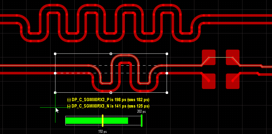
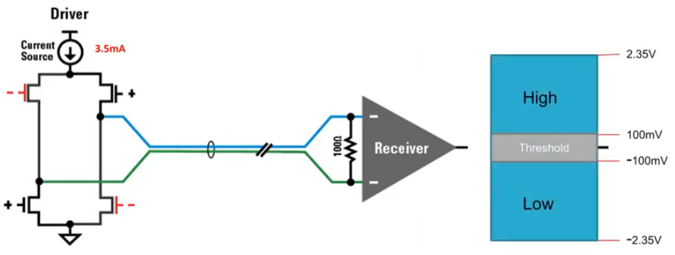
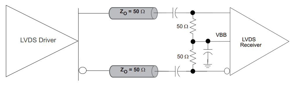
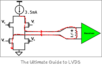
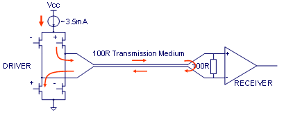
Some LVDS PCB Layout Guidelines For Ensuring Signal Integrity | PCB
 resources.altium.com
Some LVDS PCB Layout Guidelines for Ensuring Signal Integrity | PCB ...
PCB Layout Rules For PCIE, SATA, LAN, LVDS, USB, SDVO,
 www.fedevel.com
PCB layout rules for PCIE, SATA, LAN, LVDS, USB, SDVO,
Some LVDS PCB Layout Guidelines For Ensuring Signal Integrity | PCB
Some LVDS PCB Layout Guidelines for Ensuring Signal Integrity | PCB ...
General Pcb Layout Design Guidelines For Rf And Digital To Analog | My
 www.myxxgirl.com
General Pcb Layout Design Guidelines For Rf And Digital To Analog | My ...
Some LVDS PCB Layout Guidelines For Ensuring Signal Integrity | PCB
 resources.altium.com
Some LVDS PCB Layout Guidelines for Ensuring Signal Integrity | PCB ...
Some LVDS PCB Layout Guidelines For Ensuring Signal, 40% OFF
 www.oceanproperty.co.th
Some LVDS PCB Layout Guidelines For Ensuring Signal, 40% OFF
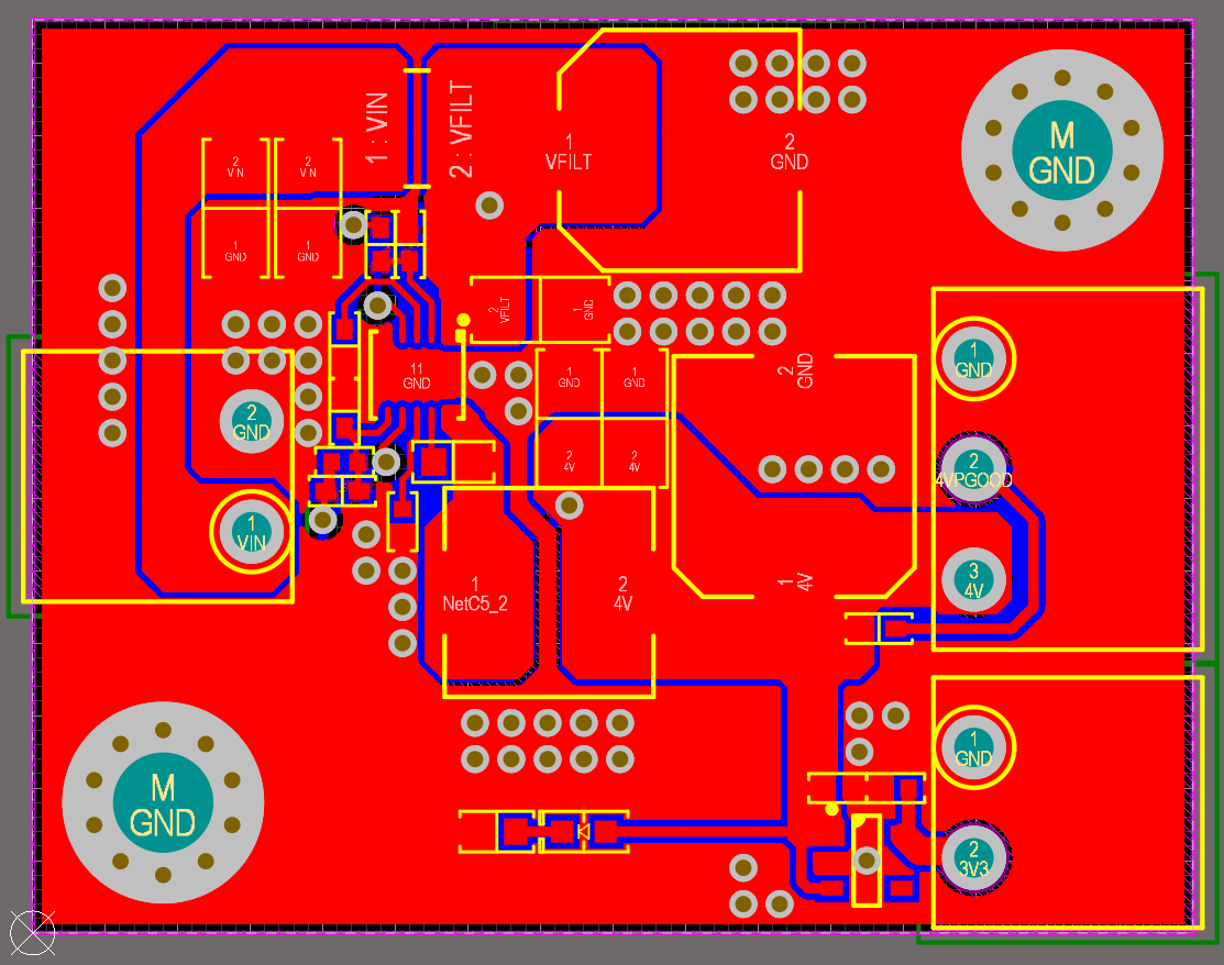
SMPS PCB Layout Guidelines In Altium Designer
 resources.altium.com
SMPS PCB Layout Guidelines in Altium Designer
Some LVDS PCB Layout Guidelines For Ensuring Signal Integrity | PCB
Some LVDS PCB Layout Guidelines for Ensuring Signal Integrity | PCB ...
Reparator Credential Dumnezeu Pcb Design Guidelines Releu Alb Ca
 cristor.dz
Reparator Credential Dumnezeu pcb design guidelines releu alb ca ...
LVDS PCB Layout – Expert Guidelines You Need To Know! Pcb Layout Design
 superspotsz.blogspot.com
LVDS PCB Layout – Expert Guidelines You Need to Know! Pcb layout design ...
Some Lvds Pcb Layout Guidelines For Ensuring Signal Integrity - EMS
 electronicmanufacturingservice.org
some lvds pcb layout guidelines for ensuring signal integrity - EMS
Altera's LVDS System PCB Board Design CloningPCB Reverse Engineering
 www.circuitengineer.com
Altera's LVDS System PCB Board Design CloningPCB Reverse Engineering ...
Some LVDS PCB Layout Guidelines For Ensuring Signal Integrity | PCB
 resources.altium.com
Some LVDS PCB Layout Guidelines for Ensuring Signal Integrity | PCB ...
(PDF) AN11088 PTN3460 DP To LVDS PCB Layout Guidelines - DOKUMEN.TIPS
 dokumen.tips
(PDF) AN11088 PTN3460 DP to LVDS PCB layout guidelines - DOKUMEN.TIPS
PCB Layout Guidelines And Considerations
 www.microcontrollertips.com
PCB layout guidelines and considerations
Some LVDS PCB Layout Guidelines For Ensuring Signal, 40% OFF
 www.oceanproperty.co.th
Some LVDS PCB Layout Guidelines For Ensuring Signal, 40% OFF
Some LVDS PCB Layout Guidelines For Ensuring Signal Integrity | PCB
 resources.altium.com
Some LVDS PCB Layout Guidelines for Ensuring Signal Integrity | PCB ...
LVDS Board Design Guidelines: Altera FPGAs & PCB Layout
 studylib.net
studylib.net
LVDS Board Design Guidelines: Altera FPGAs & PCB Layout
LVDS PCB Layout – Expert Guidelines You Need To Know! Pcb Layout Design
 superspotsz.blogspot.com
LVDS PCB Layout – Expert Guidelines You Need to Know! Pcb layout design ...
PCB Layout Guidelines For High Speed Applications - HardwareBee
 hardwarebee.com
PCB Layout Guidelines For High Speed Applications - HardwareBee
PCB Layout Guidelines For USB Type-C
PCB Layout Guidelines for USB Type-C
Some LVDS PCB Layout Guidelines For Ensuring Signal Integrity | PCB
 resources.altium.com
Some LVDS PCB Layout Guidelines for Ensuring Signal Integrity | PCB ...
PCB Design Layout Guidelines For Engineers | Advanced PCB Design Blog
 resources.pcb.cadence.com
PCB Design Layout Guidelines for Engineers | Advanced PCB Design Blog ...
Some LVDS PCB Layout Guidelines For Ensuring Signal Integrity | PCB
 resources.altium.com
Some LVDS PCB Layout Guidelines for Ensuring Signal Integrity | PCB ...
Pcb layout rules for pcie, sata, lan, lvds, usb, sdvo,. Some lvds pcb layout guidelines for ensuring signal, 40% off. Some lvds pcb layout guidelines for ensuring signal, 40% off